Semiconductor Packaging & SoC Design
2026-05-11 | By Antonio Velasco
The word "semiconductor" is a strong buzzword. They drive the stock market, enable all of our electronics and systems, and essentially hold up the world. Yet, when most people think of semiconductors, they think of the silicon chip: a tiny, intricate network of logic gates and components that make up our computers. However, the manufactured chip itself is only half the battle, and there lies a whole discipline that enables these chips to even function: semiconductor packaging.
I’ve had the opportunity to intern for semiconductor companies throughout my career and learned that packaging is far more than just placing a chip in a protective shell and on a board. Package engineering encompasses a little bit of everything: electrical, mechanical, thermal, and materials—it covers every type of engineering. This one field alone dictates performance, reliability, manufacturability, cost, and so much more. Although silicon designers get the chip designed and foundries fabricate it, packaging turns it from a random die to an actionable component.
For anybody curious or considering a career path in packaging, it is essential to understand today’s electronics as a whole.
What is Semiconductor Packaging?
Whenever I say that I work on semiconductor packaging, most people think of boxes or bags. Granted, package engineering for boxes and the like is a big thing in the industry (Rutgers even offers a degree in it), but semiconductor packages are a whole different thing. "Packaging" refers to the process of enclosing a fabricated die inside a protective system that not only keeps it active but also ensures electrical connectivity, thermal management, and integration.
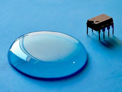
The most common thought of a semiconductor is the raw chip after it is fabricated onto a silicon wafer, or rather, the individual die. Here’s an example of the LM2576T die from Texas Instruments, a simple voltage regulator.

By itself, it’s very complex but extremely sensitive. By itself, it can’t do much and does not offer easy integration. You can see what it looks like after packaging here:

Packaging transforms this bare die into a functional electronic component. Not only that, but it also ensures mechanical support and durability, thermal management, power delivery, and overall robustness. In today’s semiconductor industry, packaging has become a system-level design discipline rather than simply a post-fabrication step.
These days, packaging is more important than ever as we get smaller in terms of fabrication. Nowadays, the limit isn’t in the gate size (as it has traditionally been), but rather in the physical limitations and manufacturing complexity of the package around it. Performance growth relies on packaging, especially in SoC design, where CPU, GPU, memory, and more separate blocks need to work together.
Considerations and Functions
Within semiconductor packaging, as mentioned, come many different disciplines. It acts as a form of system engineering and requires many different considerations.
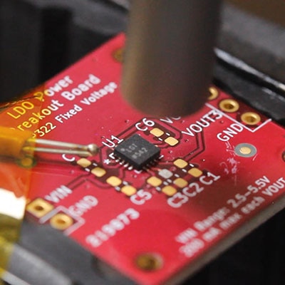
The first of which is electrical. Obviously, in order for a semiconductor die to work efficiently, its electrical connections between the silicon and the external circuitry (like that of a PCB) need to be reliable. Signals, power, data, and more need to flow through the chip efficiently. The name of the game here is the connection with the chip itself. You might’ve experienced soldering a component to a PCB—the concept is the same here. The chip must be connected to its external packaging, which can then be connected elsewhere. Wire bonding is a popular method, but flip-chip bonding may be an option as well. The main consideration comes when signal integrity is paramount, like in high-speed digital and RF applications.
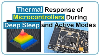
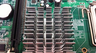
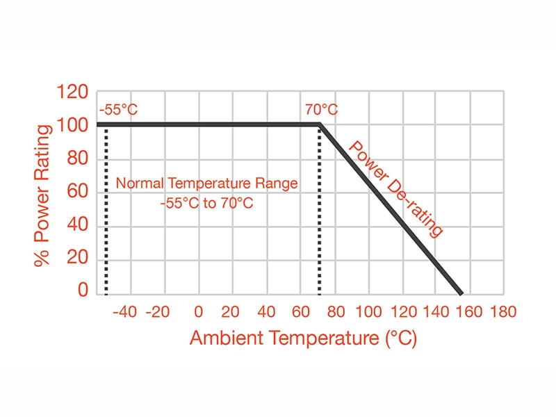
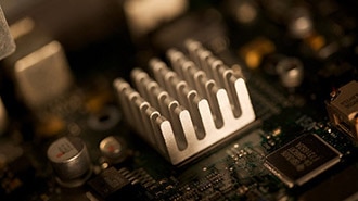
Next up is thermal management. You might notice your computer or phone gets hot after a while—that's because modern chips generate significant heat due to high transistor densities and switching speeds. Excessive temperature can degrade performance, shorten device lifespan, and cause catastrophic failure. Effective packaging can help to mitigate this, either by providing thermal pathways to remove heat and transfer it to heat sinks or to simply provide fewer “hot spots.” This means doing a ton of simulations and looking a lot into material selection. In any case, effective thermal management means better performance and reliability.

Mechanical reliability is also an important consideration, especially when we consider the fact that by itself, the silicon die is extremely fragile. When we’re talking about super small gate sizes and traces, any small amount of moisture or contamination can be an issue. This was something I focused a lot on in my previous internship, especially when it came to mechanical stress. Vibration, solder fatigue, and material cracking were topics that came up all the time.

Another common consideration is power delivery. With the size of chips these days, power delivery is becoming more and more challenging. Power blocks often litter boards as advanced processors require extremely stable and low-variety power supplies. When designing packages, power distribution must be at the forefront to prevent voltage drops and EMF. Moreover, with how sensitive dies can be, any small overcurrent or voltage spike can cause catastrophic damage.
The Interdisciplinary Nature of Package Engineering
With all of these considerations, it’s no surprise that packaging requires expertise across a variety of domains. Materials engineers develop substrates and thermal interfaces; electrical engineers ensure power delivery and EMF shielding; mechanical engineers minimize stress and vibration; and thermal engineers model heat flow and propose cooling strategies. There’s something for everybody, and mastering the domain requires a little bit of everything.
For me, this provides the perfect opportunity to get involved. I’ve always been more drawn to systems engineering and want to pursue it more in the future. What better place to be than to use my electrical engineering background to get my foot in the door and to better understand all of the other fields in the context of microelectronics?
Career Opportunities
As I mentioned, I’ve found a comfortable niche in semiconductor packaging as a package reliability engineer. This means ensuring that the proposed package design is not just viable, but also stable and efficient in terms of thermal management, electrical routing, and much more. It puts together everything I’ve loved from my classes and past experience and allows me to continue growing as an engineer. Within semiconductor packaging, there lies a variety of other careers:
- Signal Integrity Engineering
- Thermal Engineering
- Materials Engineering
- Manufacturing Engineering
- Design Engineering
There’s something for most engineers, and if you’re interested in dipping into a little bit of everything, Package Engineering provides an interdisciplinary path for you. It is a unique opportunity to influence and ensure real-world device performance and to work hands-on with physical hardware.
It's also an exciting time as we look towards incorporating photonics and increasingly more complex chip designs. With increasing global investment in semiconductor manufacturing and advanced packaging facilities, engineers entering this field can expect long-term career opportunities.
Semiconductor packaging is the true bridge between electrical design and real-world application. As transistor scaling becomes more and more challenging (we’re reaching the edge of what’s physically possible), packaging has become the primary driver of innovation. Stacking and the integration of multiple dies into one package have allowed optimization, and development is only advancing. For anybody looking to explore a microelectronics career, packaging offers both an exciting and multidisciplinary path towards shaping the future of technology.