Data Acquisition Signal Chain Simulation Simplifies Component Selection and Testing
Contributed By DigiKey's North American Editors
2025-11-24
Designing a data acquisition system used to mean searching for the right combination of components from within a ream of data sheets and troubleshooting cobbled-together prototypes. Now, designers can save time and frustration with digital design tools that enable them to drag and drop models of components like sensors, analog signal-conditioning blocks, analog-to-digital converters (ADCs), and digital filters into a virtual signal chain. The software simulates the virtual chain’s output, allowing the designer to see how the chosen components affect results such as signal-to-noise ratio (SNR), gain and offset error, and power.
Analog Devices, Inc. (ADI)’s digital design suite, Precision Studio, includes Signal Chain Designer, a module that helps designers simulate their data acquisition systems before building them. In Signal Chain Designer, a user chooses a sensor, sets parameters for the model, and then drops in circuit blocks that represent the components in the signal chain (Figure 1).
 Figure 1: The Signal Chain Designer within ADI’s Precision Studio allows designers to choose a sensor, then drag and drop circuit blocks into the chain to simulate data acquisition components. (Image source: Analog Devices, Inc.)
The sensor signal must pass through several stages on its journey to becoming reliable data, and each stage consists of one or more electronic or integrated circuit (IC) components that prepare the signal for the next stage. The most common stages amplify the analog signal, filter the analog signal, convert the analog signal to digital, and filter the digital signal.
Analog signal amplification stage
Analog signals generated by sensors often fail to match the optimum inputs of the data acquisition system. The analog signal amplification stage uses operational amplifiers (op amps), fully differential amplifiers, and voltage references, as well as passive components like resistors, capacitors, and inductors, to convert the sensor signal into an efficient form for the data acquisition system.
In Signal Chain Designer, the user specifies the analog amplification stage’s input and output types, the gain needed, and the level shift required to achieve the correct voltage input. The software then creates a circuit that meets the specified parameters using ADI products and outputs a schematic.
For instance, for the sensor utilized in Figure 1 with 1 kΩ impedance at 1 kHz and 100 pF capacitance, the user may specify a gain of 2 V/V and a level shift of 2.5 V (Figure 2).
 Figure 2: Users of Signal Chain Designer specify the configuration, gain, level shift, and other parameters of the analog signal amplification stage. (Image source: Analog Devices, Inc.)
Based on these parameters, the software builds a circuit schematic for the analog signal amplification stage (Figure 3, top) containing an ADA4097-2 op amp. Op amps in the ADA4097-2 family require only 32.5 µA per channel to achieve a 130 kHz gain-bandwidth product (GBP) for large signal voltage gain, with 1,000 nV peak-to-peak (P-P) noise between 0.1 Hz and 10 Hz and a typical 1/f noise corner at 6 Hz.
The software also develops a reference circuit for the amplifier stage with an LTC6655B-2.5 precision bandgap voltage reference and an AD8510 op amp (Figure 3, bottom), both from ADI.
 Figure 3: Signal Chain Designer’s analog signal amplification stage circuit schematics, based on user specifications and including appropriate electronic components from ADI. (Image source: Analog Devices, Inc.)
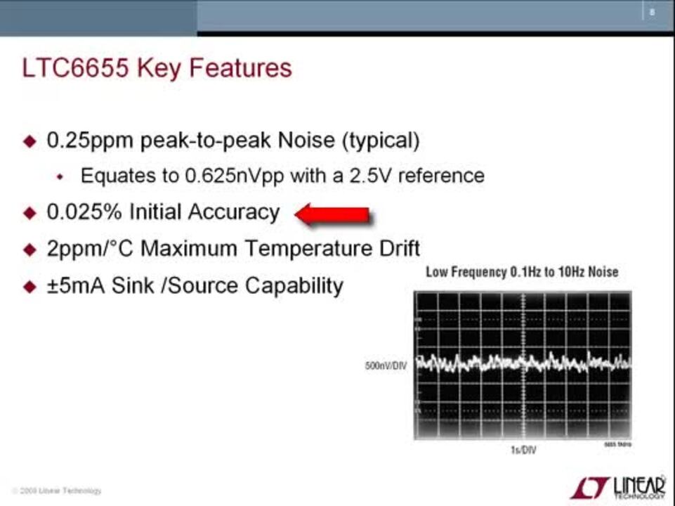
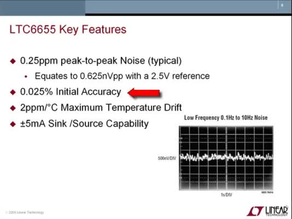
The LTC6655B-2.5 has 625 nVP-P noise for 0.25 ppmP-P between 0.1 Hz and 10 Hz, ±0.025% maximum accuracy, and low voltage drift of 2 ppm/°C maximum, ensuring it outputs a stable signal voltage regardless of variations in input voltage and load. The AD8510 junction field-effect transistor (JFET) op amp typically has 8 nV of spectral noise at 1 kHz, requires only 25 pA of input bias current, and settles to a 0.1% error band within 500 ns.
Signal Chain Designer also allows the user to specify how signals are conditioned at this stage. Users can configure fully differential amplifiers, instrumentation amplifiers, or current sense amplifiers.
Analog signal filtering stage
The amplified analog signal must next be filtered to remove noise and distortion introduced by amplification. Filters can use passive components like resistors and capacitors to create first-order filters that have gentle -20 dB/decade roll-offs after the cutoff frequency. Second-order and higher-order filters are usually active filters that employ one or more op amps to achieve sharper roll-offs.
The filter configuration will dictate whether it attenuates frequencies above the center frequency, f0 (low-pass), below f0 (high-pass), outside two cut-off frequencies (band-pass), or outside a specific band of frequencies (band-stop or notch). Other filter parameters, like Q factor, further refine filter response, defining the sharpness of roll-offs, transient behavior, and the shape of the passband.
In Signal Chain Designer, users can configure the parameters for simple filters by choosing the filter type and specifying key parameters. Signal Chain Designer’s Filter Wizard can also design simple filters through third-order and higher filters and import the filter back into the digital signal chain design. In the example (Figure 4), the user opts for a low-pass filter with an f0 of 10 kHz and a Q factor of 0.707. The selected Sallen-Key type filter uses a single op amp to accept high input impedance and output a low-impedance signal with good stability.
 Figure 4: Users define analog filtering stage parameters in Signal Chain Designer, including filter type, f0, Q factor, and gain. (Image source: Analog Devices, Inc.)
With these parameters, Signal Chain Designer outputs a circuit including ADI’s LT6020 rail-to-rail op amp (Figure 5). The LT6020 consumes less than 100 µA but can still respond quickly to changes in the input signal with a slew rate of 5V/µs. It has a GBP of 400 kHz over its -40°C to +125°C temperature range.
 Figure 5: The analog signal filter stage circuit diagram output by Signal Chain Designer specifies an LT6020 op amp with high slew rate and low power consumption as the low-pass Sallen-Key second-order filter. (Image source: Analog Devices, Inc.)
Analog-to-digital conversion stage
The final step in a signal’s journey from sensor response to data is the conversion of the analog signal into a digital form. Common ADC architectures include successive approximation register (SAR) for good resolution at a moderate sampling rate, and Delta-Sigma (ΔΣ) for high resolution at lower sampling speeds. To achieve the desired digital output, designers must know the input type, system resolution, and output data rate.
Users specify these parameters in Signal Chain Designer, and the software outputs an ADC circuit including a voltage reference and a passive resistive/capacitive (RC) filter on the input. Some ADCs also allow users to integrate digital filtering or to set the ADCs to high impedance (Hi-Z) mode for simpler, lower-power designs.
In the example (Figure 6), Signal Chain Designer’s output specified ADI’s ADR4525 voltage reference and the AD7175-2 ΔΣ ADC. The ADR4525 has good temperature stability with temperature coefficients between 0.8 ppm/°C and 4.0 ppm/°C, and output noise of 1 µVP-P at 2.048 VOUT and 0.1 Hz to 10 Hz. The AD7175-2 is a 24-bit ADC with 250,000 samples per second (250 kSPS) throughput and 20 µs settling time.
 Figure 6: In the analog-to-digital conversion stage, the Signal Chain Designer’s circuit diagram includes a passive RC input filter, a voltage reference, and an ADC module. (Image source: Analog Devices, Inc.)
In any stage of the signal chain, the user can view a product table showing appropriate alternate components. For instance, a designer may choose to substitute an SAR ADC like the AD4008 for the ΔΣ ADC shown in the example. The AD4008 draws between 70 µW at 10 kSPS and 14 mW at 2 MSPS, its maximum power. Pseudo-differential operation allows 16-bit precision with a simplified design in Hi-Z mode.
After analog-to-digital conversion, designers may optimize the output by dropping digital filter blocks into the design downstream of the ADC in Signal Chain Designer. Options in these digital filtering blocks include averages, first- and second-order filters, and simple moving-average CIC filters.
After building a virtual data acquisition system using Signal Chain Designer, users can simulate frequency response, noise, DC error budget, power, and input ranges from within the software. For more customized simulations, Signal Chain Designer can create virtual testbenches that can be edited and run in LTspice.
Conclusion
Digital tools like ADI’s Signal Chain Designer can minimize the guesswork and frustration of building a precision data acquisition system. With models of a wide variety of readily available op amps, voltage references, ADCs, and other components within the software, Signal Chain Designer lets users fine-tune their data acquisition systems virtually, ensuring a smooth transition to acquiring and deploying hardware.
Disclaimer: The opinions, beliefs, and viewpoints expressed by the various authors and/or forum participants on this website do not necessarily reflect the opinions, beliefs, and viewpoints of DigiKey or official policies of DigiKey.